


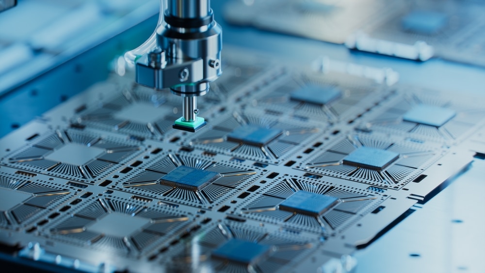
Silicon computer chips have effectively served us for over half a century. The smallest features on chips presently obtainable are about 3 nanometers — an incredibly small size considering a human hair is approximately 80,000 nanometers wide. Decreasing the size of features on chips will aid us in satisfying our unending necessity for more memory and processing power in our grasp. However, the boundary of what can be accomplished with standard materials and procedures is imminent.
Advancements in Chip Materials
Scientists at the U.S. Department of Energy’s (DOE) Princeton Plasma Physics Laboratory (PPPL) are employing their proficiency in physics, chemistry, and computer simulation to invent the succeeding generation of computer chips, striving for procedures and materials that will generate chips with smaller features.
“All our current electronic gadgets utilize chips comprised of silicon, which is a three-dimensional substance. Now, numerous businesses are making significant investments in chips fashioned from two-dimensional materials,” stated Shoaib Khalid, an associate research physicist at PPPL. The materials essentially exist in three dimensions, but they are so slender — often consisting of only a few layers of atoms — that scientists have taken to labeling them 2D.
Transition-Metal Dichalcogenides: Advanced Semiconductors
Khalid, in collaboration with PPPL’s Bharat Medasani and Anderson Janotti from the University of Delaware, probed one possible silicon substitute: a 2D material recognized as a transition-metal dichalcogenide (TMD).
Their recent document, published in the periodical 2D Materials, delineates the inconsistencies that can arise in the atomic arrangement of TMDs, the reasons for their occurrence, and how they impact the material. Insight into these variations lays the foundation for enhancing the procedures necessary to fabricate next-gen computer chips.
In essence, the objective is to devise plasma-based manufacturing systems capable of producing TMD-based semiconductors tailored to the precise criteria essential for the application.
TMD: A Minute Metal Layer Cake
A TMD can be as slim as three atoms tall. Think of it akin to a petite metal layer cake. The outer layers consist of a chalcogen element: oxygen, sulfur, selenium, or tellurium. The filling comprises a stratum of transition metal — any metal from groups 3 to 12 in the periodic table of elements. A bulk TMD encompasses five or more strata of atoms. The atoms are organized in a crystalline framework or lattice. Ideally, the atoms are structured in a meticulous and uniform pattern across the lattice. In actuality, minor deviations can be discerned in the pattern. A specific location in the pattern might lack an atom, or an atom might be located in an unusual position. Scientists term these deviations imperfections, but they can have a beneficial influence on the material.
Certain TMD imperfections, for instance, can heighten the semiconductor’s electrical conductivity. Regardless of their nature, it is crucial for scientists to comprehend why imperfections arise and how they will impact the material so theyYou can integrate or remove these flaws accordingly. Familiarity with typical imperfections also enables scholars to provide rationale for the outcomes of prior trials involving TMDs.
“Upon the production of bulk TMDs, an excess of electrons is detected,” Khalid remarked, noting that the cause of these surplus negatively charged particles remained uncertain for researchers. “In our study, we propose that hydrogen might be accountable for the surplus electrons.”
After computing the energy needed to generate various types of TMD defects, the researchers arrived at this deduction. They scrutinized defects related to chalcogen vacancies, which were previously acknowledged as existing in TMDs, as well as defects associated with hydrogen due to its common presence in the chip manufacturing process. The researchers are particularly keen on discerning the defects that demand minimal formation energy, as these are the ones more liable to manifest — they need minimal energy to occur!
Subsequently, the team explored the influence of each defect type with low formation energy. Specifically, they aimed to comprehend how each defect arrangement could impact the material’s electrical charge. It was discovered by the researchers that one defect configuration involving hydrogen produces extra electrons, resulting in a negatively charged semiconductor material known as an n-type. Computer chips are made utilizing blends of n-type semiconductor material and positively charged, or p-type, material.
Research Observations on Chalcogen Vacancies
The alternate class of imperfection scrutinized in the document is recognized as a chalcogen vacancy: a missing atom of oxygen, sulfur, selenium, or tellurium, contingent on the TMD type. The researchers concentrated on clarifying the outcomes of earlier assays on fragments of the bulk TMD substance molybdenum disulfide. The experiments, which entailed illuminating the TMD, unveiled unexpected light frequencies emitted by the TMD. The researchers established that the unexpected frequencies were attributable to the movement of electrons linked to the chalcogen vacancy.
“This is a prevalent flaw. It is frequently discernible from scanning tunneling microscope images when producing the TMD layer,” Khalid expressed. “Our study offers a technique to scrutinize the presence of these vacancies in the bulk TMDs. We elaborated on previously observed experimental findings in molybdenum disulfide, and then we anticipated a comparable outcome for other TMDs.”
The methodology recommended by the researchers entails evaluating the TMD for defects employing measurement methods known as photoluminescence to determine the light frequencies emitted by the material. The peak frequency of light can be leveraged to ascertain the electron configurations of the atoms in the TMD and the existence of chalcogen defects. The log article encompasses information regarding the frequencies that would be emitted by five types of TMDs with chalcogen vacancies, incorporating molybdenum disulfide. Consequently, the findings offer a blueprint for examining chalcogen vacancies in forthcoming trials.
Image Source: IM Imagery / Shutterstock